FUNDAMENTAL INVESTIGATION OF CHARGE TRANSPORT AND RECOMBINATION IN WIDE BAND GAP MATERIALS BY NOVEL METHODS
15. Aims, significance and expected outcomes.
Acknowledgments
This proposal is based on an earlier proposal that was well rated at an average of 84.4 (excellent) but did not cross the threshold of 89 required for funding in 1998. After counsel with senior colleagues and further work, we respectfully submit this substantially refocused proposal for funding in 1999. We are grateful for the assistance provided by our collaborators in the preparation of this proposal. We also wish to acknowledge the Faculty of Science that provides a substantial infrastructure support for this project. This allows us to request funds from the ARC that may seem modest in relation to the goals of the proposal by US, Japanese or European standards. A copy of this proposal, with additional colour diagrams, appears at: http://www.ph.unimelb.edu.au/~dnj/ibic.html
Introduction and proposal summary
Wide band-gap materials show considerable promise for microelectronics applications in extreme and hostile environments for radiation hard detectors and low noise circuit elements. These applications exploit the fact that the promotion of charge carriers across the wide band gap is difficult, making the materials relatively insensitive to temperature or ionising radiation. This attribute of the materials also makes them challenging to study. The promotion of charge into the conduction band for charge transport cannot readily be accomplished by conventional sources of excitation. Nor can conventional sources of excitation be readily used to produce high-resolution images of the associated structures. No such problem exists with focused MeV ions.
This proposal, therefore, aims to exploit the unique ability of focused MeV ions to inject charge deep into the materials so that important charge transport characteristics can be measured. The charge transport properties of greatest interest are the charge drift, diffusion and funnelling. The phenomenon of funnelling occurs when the passage of ionising radiation through the material creates a plasma column. This momentarily increases the volume of the depletion region in a microelectronic device which could increase its charge collection efficiency and increase its susceptibility of a single event upset where the surrounding circuit can change its state.
The influence of defects on these essential properties is the focus of this proposal. In fact, the effect of defects in wide band gap materials, which often appear as extra levels in the band gap, has been identified in the literature as the single most significant barrier to the application of wide band gap materials to practical devices.
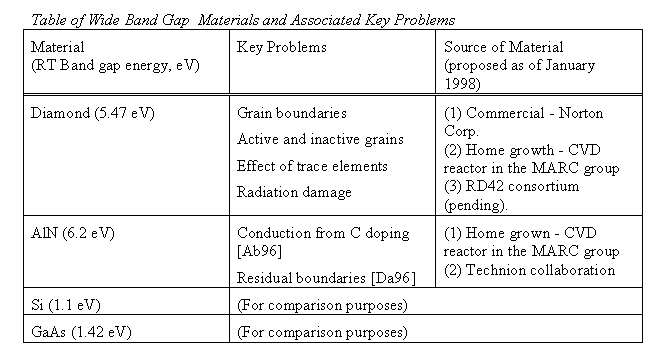
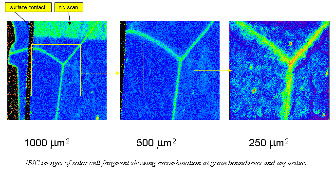
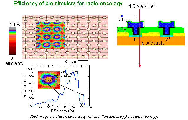
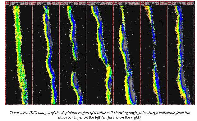
We first aim to study the mechanism of the charge injection process from MeV ions. We plan to exploit the Ramo mechanism (discussed below), already proven for some studies of diamond, and apply it to important problems in selected materials. The materials are listed in the table below with the specific characteristics that we plan to investigate. Our novel techniques can provide valuable information that cannot be obtained by conventional techniques. One of our established techniques, called IBIC (Ion Beam Induced Current), measures the charge collection efficiency of materials. Another established technique, called IL (Ionoluminescence), measures the radiative transitions that occur across levels in the band gap. These two methods have been proven on the study of diamond (see below). We now plan to develop a new technique, called Scanning Ion Deep Level Transient Spectroscopy (SIDLTS) to measure the trap levels in the band gap contributed by defects. Taken together, these three techniques, performed simultaneously on the same region of interest, can image the distribution of defects and identify which are electrically active. This can be related to electron and hole mobilities, lifetimes, radiation hardness and other fundamental properties of the materials. As a prototype of the study of the wide band gap materials, we applied these techniques to solar cells (see figure below). Here the mechanisms of charge transport and recombination are much better understood, but where the irradiation by MeV ions still led to useful and unique information being obtained (see progress reports).
Aims
This work builds on our extensive experience with the use of focused MeV ion beams for materials characterisation. Not only does this project address the most important problems in the physics of synthetic wide band gap materials, but also plays a leading role in maintaining the MARC group at the forefront of nuclear microprobe research.
Significance and Expected Outcomes:
16. Research plan, methods, techniques and proposed timing.
We first discuss the features of the individual materials in our list of key materials that we plan to investigate, then continue with a discussion of the novel analytical techniques we plan to apply to these features. We also discuss the advantages of our approach over the competing techniques. The techniques to be used by us are referred to by their acronyms listed here for convenience: IBIC: Ion Beam Induced Current, CCM: Channeling Contrast Microscopy, IL: Ionoluminescence
16.1 Research Plan for Individual materials
Diamond: Our research group has already done a substantial amount of preliminary work on the characterisation of diamond by our IBIC technique. Indeed, we plan to apply many of the techniques developed for diamond to the other wide band gap materials, in particular AlN, identified in this proposal. Diamond is presently being intensively studied for radiation hard detectors in adverse environments including high-energy physics experiments [Ba95, Wh94]. In addition, undoped diamond has extremely high resistivity and high breakdown field strength offering excellent electrical isolation together with high electron and hole mobilities. Furthermore, diamond is regarded as an inert, biocompatible material with a low atomic number that is closely matched to human tissue making it ideal for radiation dosimetry applications [Ka93].

To successfully use diamond as a radiation detector, it is necessary to fully characterise the charge transport, recombination and collection mechanisms. Recently, high quality synthetic diamonds have become available. These are polycrystalline with a grain size of ~50 mm so the nuclear microprobe is ideal for performing IBIC analysis on these materials. Considerable IBIC work on commercial films has been done by the group of Manfredotti et al. (see e.g. [Ma96]) in collaboration with the nuclear microprobe group in Zagreb.
The mechanism for the production of IBIC signals from diamond films is illustrated in the figure above. The diamond film, typically 250 to 400 mm thick, is configured in the Metal-Insulator-Metal (MIM) configuration. Ion beams may be incident from the surface (normal IBIC), which is also the growth direction, or from the transverse direction (lateral IBIC). A bias voltage to provide an electric field is necessary for the detector to function. The mechanism for charge generation in the external circuit is by induction due to the movement of the electron-hole pairs under the influence of the electric field. This is described by Ramo’s theorem and its generalisations [Ra38, Ca63, Ca71]. Defects and other inhomogeneities can rapidly trap charge allowing it to recombine. This reduces the amount of charge otherwise available in the external circuit. The IBIC images are very sensitive to distribution of these defective regions in the diamond. We propose to extend IBIC imaging through the Ramo mechanism to other semiconductors, in particular AlN.
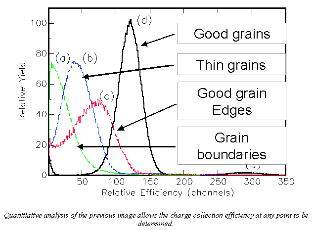
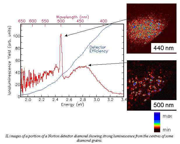
Some representative normal IBIC images obtained in Melbourne were presented by Beckman et al. [Be97] at a recent international conference and by DNJ at the Hiroshima@Melbourne conference on detectors for high energy physics experiments. Complete understanding of the IBIC images is complicated by a variety of phenomena including transient polarisation of the matrix by the beam or the bias voltage and effects arising from properties of the metal-diamond contact. However, the IBIC images display considerable structure indicating about three times more efficient charge collection from the centre of the diamond grains compared to the grain boundaries. Very low efficiency (~1/10 of grain centres) was observed from regions not covered by the metal contacts. This last result is quite different to the situation for most IBIC work to date on semiconductor materials and devices [Br96] where the specimen usually incorporated a depletion region.
The ionoluminescence [Be97a] spectrum of the IBIC specimens displays features typical of high quality CVD diamond films. The two peaks seen in the IL spectrum show strong luminescence at 440 nm from the centres of the grains, with more uniformly distributed luminescence at 500 nm. We attribute the different luminescence from grain boundaries to the presence of defects that provide some non-radiative recombination pathways. Detailed comparison of the IL and IBIC spectra from the same regions of the diamond films may provide additional insights into the charge transport and recombination mechanisms and will be the focus of the present proposal for diamond. We plan to extend this work to fully account for the effects that have major implications for the use of diamond as a radiation detector.
AlN: This new material has been proposed as a very promising material for integration into conventional electronic devices, mainly because it will grow on a variety of substrates. Also, conductive AlN has been produced by 8% C doping, the conduction mechanism is still a matter of investigation, but is possibly due to filamentary conduction paths [Ab96]. High-resolution non-Rutherford backscattering spectrometry, combined with IBIC will readily determine if this is true. Conductive AlN would have many important applications in GaN/SiC devices. In the growth of thick films of AlN, the coalescence of islands of initial nucleation produce double positioning boundaries [Da96]. The concentration of these boundaries in the final film strongly influences its quality. We will determine the effect of these residual boundaries on the film quality by means of IBIC. We plan to synthesize AlN within our own laboratory and pilot experiments have shown that this is possible. In addition, we have a student participating in an exchange program with the Technion, Israel, where high quality AlN films are grown.
Advanced studies: The above important issues are all involved with the structure and growth of single compound films. Problems that are more complex arise when films are combined into multilayers, such as is done to make heterojunctions. The quality of the interface is of crucial importance in the construction of p-n junctions in working microelectronic devices. One of the characteristics of a p-n junction is the presence of a depletion region where free charge is swept from the lattice by the built-in electric field. We propose to investigate the formation of depletion regions in heterostructures from low-grade materials. We anticipate that the IBIC signal, from charge carriers injected into the junction by the ion beam, will be readily collected from contacts from regions containing depletion regions. We propose to use this signal as a means to identify the formation of AlN/diamond junctions with a depletion region. The success of this idea would have major implications for determining the success, or otherwise, of attempts to make devices from diamond.
16.2 Research Plan for Methods and Techniques
Review of Competing Techniques: Many competing techniques have been used for the electrical and band-gap analysis of materials and devices. One widely used technique is Electron Beam Induced Current (EBIC). This technique is an imaging mode on a scanning electron microscope. An EBIC image is formed by using the specimen as a detector or "collector" of the electron beam induced current. EBIC measures a steady-state current from the electron probe and can only be used for transient studies if beam blanking is available on the microscope. EBIC can also suffer from large beam broadening that adversely effects the spatial resolution for buried device structures. IBIC was developed to overcome some of these problems. The heavier, higher energy charged particles used in IBIC allow greater penetration of the specimen, without spatial broadening, and a greater amount of charge produced per incident particle. This means that for IBIC imaging it is possible to measure the charge from individual particles and thus study very rapid charge collection transients in the specimen.
Photoluminescence (PL) has been used for the analysis of band-gap structure in semiconductors. Most PL is preformed with visible or IR lasers and therefore cannot be used to excite transitions in wide band-gap materials. The electron microscope technique of Cathodoluminescence (CL) could be used to excite these transitions but the electron scattering leads to degradation in spatial resolution. Ionoluminescence (IL) suffers from far less scattering than CL and has a greater luminescent yield per particle. From these above arguments, we have proposed that the Ion Beam characterisation techniques provide considerable flexibility and rival the current conventional techniques.
Our Novel Techniques: A full discussion of these techniques may be found in: Materials Analysis with a Nuclear Microprobe by M.B.H. Breese, D.N. Jamieson and P.J.C. King, Wiley, 1996. We briefly introduce them here.
Ion Beam Induced Charge (IBIC): IBIC is a technique that was originally developed for the imaging of electronically active microscopic regions in integrated circuits. More recently, the technique is finding wider application in the study of basic charge transport properties of, not only integrated circuits, but also simple novel material structures. The technique utilises the movement of charge created by MeV ions passing through in the test sample. The movement of charge is initiated by electric fields that are applied to the sample. By measuring the amount of charge collected, it is possible to gain an understanding of the collection efficiency of the structure under test. The time taken to collect the charge can also provide information about carrier mobilities and charge diffusion. This can supply data on the electronic dopants and other defects present in the crystal.
Once a material has been electrically characterised, it is then fabricated into useful devices. The fabrication of modern devices often entails the construction of multilayer and overlayer structures. IBIC is one of the only techniques that can be used to spatially resolve these buried structures and measure their electronic properties. IBIC can routinely provide 100nm spatial resolution which is adequate for the structures proposed here.
Single Event Upsets (SEU): Electronic devices present on communications satellites and other space vehicles are required to be extremely radiation hard due to the large cosmic ray backgrounds they encounter above the atmosphere. These cosmic rays can cause "single event upsets" (SEU) in these electronic devices [Pi78]. An SEU occurs when enough charge is deposited in a digital device to cause a change-in-state of the digital information being processed by the device. By appropriate device design and material selection these devices can be radiation "hardened" to give them immunity from, so called "soft errors" [Se95]. Wide band-gap semiconductors make ideal materials for these radiation hard devices.
As the size of device structures on integrated circuits becomes smaller so does the amount of charge that is used for a single bit. This means that high-density devices used at sea level are also susceptible to SEU from natural background. To characterise these high density, sub-micron devices there is a need for greater microprobe resolution. At MARC, we are working on increasing the resolution of IBIC to the nano-metre region.
To characterise these SEU's we need to use ions that have a wide range of Linear Energy Transfer (LET) [Wa88]. The light ion microprobe in Melbourne can be used for high resolution scanning with protons and alpha-particles, but the LET of these ions is too low to investigate SEU's in wide band-gap semiconductor devices. Therefore, the light ion work at Melbourne needs to be complemented with work using heavier ions. The heavy ion microprobe at JAERI Takasaki is the ideal place to perform this work. MARC has built extensive contacts with JAERI Takasaki and other Japanese laboratories. The use of these facilities has already been approved by the Japanese government and work commenced in 1998.
Scanning Ion Deep-Level Transient Spectroscopy (SIDLTS): This is a new technique we propose to develop for this project. The existence of impurities and intrinsic defects in a semiconductor greatly alter the electrical characteristics of a device through their activation in the form of discrete deep levels in the bandgap. For indirect semiconductors like Si these levels act as efficient non radiative recombination centres affecting carrier concentrations and lifetimes. Many techniques exist for characterising deep states in samples. Typically, they involve the direct generation of carriers via electrical, thermal, laser or electron beam. The Deep Level Transient Spectroscopy (DLTS) technique, introduced in the 1970's [La74], has become the standard technique for investigating non-radiative centres, whilst photoluminescence appears to be the standard for radiative ones. Normal DLTS is a bulk technique typically relying on the capacitance transient associated with the recovery of a space-charge region to a trap filling pulse and as such no correlation between the defect and its location can be made. A Scanning DLTS technique was later developed and was extensively reviewed by Leamy [Le82] where the electron beam of a SEM is used to inject charge spatially across the device.
Over the last few years MARC has been developing Scanning Ion DLTS [La96] where a focused beam of MeV light ions (protons or alpha-particles) is used to create a charge transient in a device at a given temperature. In the case of Scanning Ion Deep Level Transient Spectroscopy (SIDLTS) the energy loss of the ion through the devices presents the generation profile. Unlike DLTS and Scanning DLTS, SIDLTS recovers detrapping information as a function of temperature using the transient current integrated in an external circuit. By the use of high-speed electronics, it is possible to capture and analyse these transients. SIDLTS can be used to analyse samples where no change in the depletion thickness occurs with bias. The technique is well suited to analyse both in-grown defects and post-annealing processes in wide band gap materials like diamond. SIDLTS is virtually the only technique that can be used to characterise traps in fully depleted (insulating) materials such as diamond and AlN.
Ionoluminescence (IL): Ionoluminescence (IL) relies on the promotion of electrons to trapping levels in the band-gap. These electrons then de-excite and a photon is emitted. The wavelength of this photon is a measure of the dopant or trapping level in the material. For wide band-gap materials, it is necessary to provide the required energy to promote these electrons. IL offers this energy deposition and provides data on the radiative transitions in the material (see [Br96], ch 4 for full details). As outlined above, this method is extremely promising when applied to diamond, and several international laboratories have now followed our example and are installing apparatus for IL imaging. We hope to be the first to exploit IL for the materials in the table above.
Other Techniques: Obviously, no one analytical technique can provide all the answers. The results from the above studies fit within a larger program of analysis with a variety of other instruments. In general, these instruments are located within the laboratories of our collaborators who provide the materials. Those laboratories are listed in the above table. Thanks to our close working relationship with our collaborators, due partly to the exchange of students and staff, we have access to the measurements from the necessary complimentary techniques.
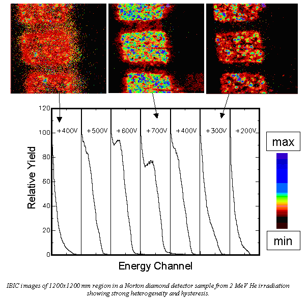
Ion Beam Damage: This is an important issue for analytical techniques involving MeV ions. This issue has received intensive attention in the past and is now well understood. Diamond is remarkably resistant to ion beam damage, at least as measured by IBIC and the other techniques of this proposal. A brief review of the major issues is covered in [Ja97]. The prior studies of this topic give us confidence that damage will not be a barrier to making the measurements proposed here.
16.3 Research Plan for Proposed Timing.
1998: Pilot studies. Application of IBIC and IL to diamond with the aim of understanding the Ramo mechanism for the induction of charge in external circuits. Preliminary characterisation by IBIC on diamond and solar cell devices. AI Saint to work for 3 months in Japan.
1999: Characterise ion solid interaction and apply models. Perform IBIC, IL and commence investigation of use of SIDLTS on both synthetic poly- and natural diamond. Investigate the extension of the Ramo mechanism to AlN from commercial sources. Obtain prototype AlN films from the Technion collaboration. On visit to Japan, perform complimentary studies with heavy ions. Obtain maps of IL and IBIC efficiency and identify electrically active defects.
2000: Irradiate materials as thin films and map charge collection efficiency. Develop Ramo mechanism-based imaging for AlN and diamond. Part of this work done in Japan (JAERI) to utilise heavy ion microprobe facilities to enter the high LET regime. Study the funnelling process in devices using heavy ion irradiation.
2001: Study defects and radiation hardness of materials fabricated into devices. Commence investigation of diamond/AlN heterostructures to investigate depletion regions formed at the interface of wide band gap materials. Conclude study of SEU devices.
17. Relevance of applicant skills, training and experience to the project.
The Chief Investigator has more than ten years experience in the use of focused MeV ion beams in the characterisation of semiconductor materials. This project represents one of the major activities of his research group that supports 5 PhD students engaged in the use of IBIC for their research projects. Thus the CI and group have considerable experience in the field. The CI has also spent several periods as a visiting fellow advising other groups on the use of these techniques in the analysis of semiconductor materials.
18. Role of each Team Leader or Chief/Partner Investigator in the proposed research; role of any other participant/s.
Role of Chief Investigator David Jamieson:
Role of the Associate Investigator Andrew Saint:
Role of Associate Investigator Steven Prawer:
Role of proposed Senior Research Fellow:
The proposed SRF is to be the key partner in the present project. The role for this fellow is:
Role of proposed Postgraduate Research Student:
19. Explanatory statement of track record, relative to opportunity.
Associate Professor and Reader in Physics David Jamieson heads the Micro- Analytical Research Centre (MARC) within the School of Physics. He is a world recognised expert on the use of focused MeV ion beams for materials modification and analysis. He is a co-author of the definitive text on the topic (Materials Analysis with a Nuclear Microprobe, Wiley, New York, 1996). He is also the author of over 80 refereed research publications on the topics of this proposal and is regularly invited to review the field at international conferences, including the Sixth International Conference on Nuclear Microprobe Technology and Applications held in Sante Fe, New Mexico in November 1996 where the topic of his work was identified by the international organising committee as the hot topic in the field. He also presented the opening plenary address at the Ion Beam Analysis conference in Lisbon in July 1997.
In addition to ARC grants, he has also negotiated contracts with some of Australia’s biggest industries, including Kodak Australia, Telecom/AOTC and Argyle diamond mines. In addition to his research output, he has also pioneered the use of his current research results in undergraduate teaching and held a substantial CAUT grant for this purpose and Universitas 21 fellowship. He has also considerable expertise in the management of large projects and currently supervises the maximum number of research students allowed by the Faculty of Science at the University of Melbourne. All of those students hold postgraduate scholarships.
20. Justification of the budget.
Personnel: This project depends on the high level collaboration established by Dr Andrew Saint between the MARC group and the two groups in Japan. The MARC group is unique in the world in having a state-of-the-art nuclear microprobe system, in house diamond/wide band gap materials fabrication equipment. The Japanese groups give us access to their experimental devices fabricated from wide band gap materials and their heavy ion irradiation facilities. Another key to the success of this project is having a central person who is familiar with all the facets of the project to work in the laboratory and also to assist with the supervision of the five PhD students whose projects for part of this proposal.
Our preferred candidate for this position, Dr. Andrew Saint performed pioneering work in developing IBIC as well as other low beam current techniques. Over the last 10 years Dr. Saint built the extensive contacts with the Japanese laboratories with whom we propose to collaborate and has been invited on a many previous occasions to work at these laboratories at the expense of the Japanese government. Through these contacts he has secured access to the facilities of their laboratories, including the TIARA (Takasaki Ion Accelerators for Advanced Radiation Application) facility in Japan. This facility will provide high energy heavy ion microbeams for SEU studies. The Takasaki group has extensive expertise in SEU studies. This proposal is asking for funding for Dr. Saint's position to utilise his expertise and international contacts to bring the research to fruition. An experimentally-oriented postgaduate student (who often narrowly miss out on a scholarship) will be sought for participation as detailed above.
Equipment: Surface barrier detectors are required for the calibration of the IBIC experiments to give quantitative results. Our methodology requires that the detectors be exposed to the primary beam from the accelerator that, unfortunately, ultimately leads to the destruction of the detectors, hence the need to replace them each year. To interface the IBIC specimens to the data collection system we also need high quality preamplifiers with superior attibutes compared to our existing preamplifiers. We propose to use an external low noise preamplifier (ORTEC 142C) which is a lower noise version of our exisiting preamplifier, but we also wish to experiment with an AMPTEK unit which can be physically mounted inside the vacuum system leading to still lower noise levels. Reduction of noise is a significant factor in obtaining high quality results, since we have found that the signal to noise level from specimens that exploit the proposed Ramo mechanism, is lower than conventional specimens which incorporate a depletion region.
Materials: Some of the materials we wish to study need to be purchased or manufactured by our collaborators. These materials also need to have electrical contacts fabricated on them. We have estimated the minimum area of crystal wafers that will allow us to obtain IBIC images in all readily available polytypes of AlN and one natural diamond window for the studies on this material.
Travel: Over each of the past 6 years, DNJ has been consistently invited to review his work and the field of materials analysis with MeV ion microprobes. We therefore request a contribution towards the airfare and living expenses for the following conferences: Nuclear microprobe technology and applications conference (2000), MRS fall meeting (Boston, U.S.A., 1999) and a third conference in 2001 (to be decided). We (with our associate investigator, Assoc. Prof. Steven Prawer) have also put in a bid to hold the conference Diamond 2000 here in Melbourne where results from this work will be presented. The field work component is requested to allow one trip each year for AS to visit our Japanese collaborators. In year one this is to participate in the heavy ion irradiation, to be followed by light ion IBIC work in Melbourne on the same specimens. In year two this is to perform heavy ion IBIC on the heterostructures and in year three this is for SEU measurements at the conclusion of the project (see also time table above). An additional visit each year will also be sought from the Japanese government who provided funds for such a visit in 1998.
References Cited in the Proposal
[Ab96] C. Abernathy and T. Strite, MRS Fall 96 Meeting GaN Symposium Highlight Summary, http://nsr.mij.mrs.org/news/symsum.html
[Ba95] C. Bauer et al. (the RD42 collaboration) Nucl. Instr. Meth. A367 (1995) 202 & 207.
[Be97] D.R. Beckman, D.N. Jamieson, S. Prawer, A. Saint and P. Gonon, Nucl. Instr. Meth. In Phys. Res. B130 (1997) 518.
[Be97a] A.A. Bettiol, K.W. Nugent and D.N. Jamieson, accepted to appear in Nucl. Instr. Meth. B (1997).
[Br96] M.B.H. Breese, D.N. Jamieson and P.J.C. King, Materials Analysis with a Nuclear Microprobe, Wiley, New York (1996).
[Ca63] G. Cavalleri, G. Fabri, E. Gatti and V. Svelto, Nucl. Instr. Meth. 21 (1963) 177.
[Ca71] G. Cavalleri, E. Gatti, G. Fabri, and V. Svelto, Nucl. Instr. Meth. 92 (1971) 137.
[Da96] R.F. Davies, S. Tanaka and R.S. Kern, J. Crystal Growth 163 (1996) 93.
[Ka93] D.R. Kania, M.I. Landstrass, M.A. Plano, L.S. Pan and S. Han, Diamond and Related Materials, 2 (1993) 1012.
[La74] D. V. Lang, J. Appl. Phys. 45(7) (1974) 3023-3031.
[La96] J. S. Laird, R. A. Bardos, G. R. Moloney, A. Saint and G. J. F. Legge, Nucl. Instr. and Meth. B106 (1995) 1114-1117.
[Le82] H. J. Leamy, J. Appl. Phys. 53 (1982) R51-R80.
[Ma96] C. Manfredotti, F. Fizzotti, E. Vittone, M. Boero, P. Polesello, S. Glassini, M. Jakšic, S. Fazinic and I. Bodganovic, Nucl. Instr. Meth. B109 (1996) 555.
[Pi78] J.C. Pickel and J.T. Blandford, Jr. IEEE Trans. Nucl. Sci. NS_25(6) (1978) 1166-1171.
[Ra38] S. Ramo, Proc. I.R.E., September (1938) 584.
[Se95] F. W. Sexton, K. M. Horn, B. L. Doyle, M. R. Shaneyfelt and T.L. Meisenheimer, IEEE Trans. Nucl. Sci. NS-42(6) (1995) 1940-1947.
[Wa88] R. S. Wagner, N. Bordes, J. M. Bradley, C. J. Maggiore, A. R. Knudson and A. B. Campbell, IEEE Trans. Nucl. Sci. NS-35(6) (1988) 1578-1584.
[Wh94] C. White, Nucl. Instr. Meth. A352 (1994) 217.
[Za95] A.M. Zaitsev, Ch XIII in Optical Properties of Diamond, FernUniversitat GHS in Hagen (1995), private publication.