We propose to create
this array using ion implantation as part of the top-down approach
now under development in collaboration with other Centre personnel.
An essential technology is the registration of single ion impacts.
We are working on two strategies for the registration.
The first strategy
involves the broad beam implantation of low dose phosphorous
ions. In this strategy the implantation of ions is essentially
randomly positioned, so the yield of usefully-spaced atoms is
low. The problem can be reduced if the passage of a single ion
can be registered so that usefully positioned ions are identifiable.
This can be accomplished by implantation of the ions through
a thin surface layer consisting of a resist. Changes to the
chemical and/or electrical properties of the resist will be
used to mark the site of the buried ion. For chemical changes,
the latent damage can be developed and the atomic force microscope
(AFM) used to image the changes in topography. Alternatively,
changes in electrical properties (which obviate the need for
post irradiation chemical etching) can be used to register the
passage of the ion using scanning tunneling microscopy (STM)
the surface current imaging mode of the AFM.
The second strategy
involves low dose rate ion implantation through a precision
mask that can be positioned at the desired locations on the
silicon substrate. In this "step-and-repeat" process, the arrival
of a single ion is registered by the electronic transient induced
in the sample itself. This method draws on our extensive experience
with the analytical technique of Ion Beam Induced Charge (IBIC)
which is used with a scanned, focused MeV ion beam for measurement
of the electrical characteristics of electronic devices such
as integrated circuits, poly-silicon solar cells and other electronic
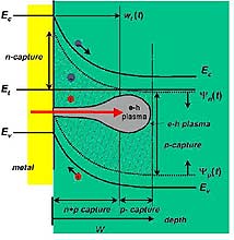
materials. The figure below shows the formation of the charge
transient from an implanted ion (red arrow) in a silicon substrate
where a Schottky barrier has been used to form a surface depletion
region.
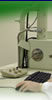
In early 2001 a 10
keV P ion implanter was commissioned for pilot studies of the
technology of the two strategies. A novel feature of this implanter
is its installation on the preparation chamber of our existing
Joel atomic force microscope. This allows atomic resolution
imaging of the implanted ions without having to transfer the
specimens to a separate instrument.